Nanomaterials lab at CU helps students, businesses focus on smallest details
BOULDER – Nanotechnology, sometimes dubbed the next industrial revolution, is expected to impact almost every aspect of our lives, including health care, communications, consumer products and electronics.
The University of Colorado at Boulder is aiming to be at the cutting edge of the revolution by launching the Nanomaterials Characterization Facility, located in the Discovery Learning Center at CU-Boulder.
The goal at the facility is to educate students and develop new technologies by attracting researchers from CU and other research institutions. It also serves as a lab for companies to conduct research using instruments they don’t have the resources to buy.
SPONSORED CONTENT
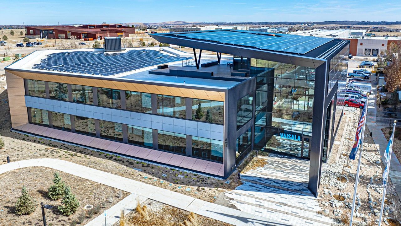
Commercial Solar is a big investment, but not an overwhelming one
Solar offers a significant economic benefit for commercial property owners while also positively impacting the environment and offering a path to compliance for new municipal requirements like Energize Denver. A local, experienced solar installer will help you navigate the complexities of commercial solar to achieve financial success for your project.
CU built the center using $1.53 million raised through a Defense Advanced Research Projects Agency grant, the National Institute of Standards and Technology and industrial sponsors GE, Ibiden USA, Lockheed Martin, Raytheon and WiSpry. Additional sponsors are being encouraged to come on board.
The $1.53 million will cover first-year research expenditures; those costs are expected to reach more than $10 million within six years.
Mechanical engineering professor Y.C. Lee directs the facility, and NIST researcher Paul Rice is facilities manager.
Rice has a joint appointment with NIST and CU because he works on similar projects at both places, he said. His specialty is carbon nanotubes – cylindrical carbon molecules on the order of 10 nanometers with properties that make them potentially useful in extremely small-scale electronic and mechanical applications because they are very strong and have unique electrical properties.
“Probably the closest thing to commercialization is mixing them in epoxy for strengthening,” Rice said. Carbon nanotubes are being used as a replacement for carbon fibers that are used in carbon composites such as tennis rackets, he said.
Rice is working on measuring the electrical and mechanical properties between carbon nanotubes and “the macro world,” he said. “So if you glue these onto a surface I want to see how strong they are.”
The direction he’s heading has to do with eventually replacing electrical circuits with carbon nanotubes because they are very good electrical conductors that don’t generate as much heat as the current technology.
Rice works at the facility part time to help students and researchers use the equipment. Instruments include:
_ Nanolithography and nanomanipulation system, an atomic force microscope that can measure surface characteristics of materials and be used for nanoindentation and nanoscratching;
_ Nano indenter, a device that provides a fast, reliable way to acquire mechanical data on the submicron scale;
_ Low-vacuum scanning electron microscope, a scanning electron microscope with a low-vacuum mode that allows users to look at specimens that cannot be viewed at high vacuum due to water content or nonconductive surface;
_ Field-emission scanning electron microscope, a scanning electron microscope that incorporates an ultra-high vacuum; and
_ Confocal laser scanning microscope that allows users to optically section a fluorescent sample (such as a cell stained with contrasting fluorescent dye) and assemble a 3-D reconstruction of the entire sample.
The facility hopes to add an X-ray photo electron spectrometer, focused ion beam and transmission electron microscope.
Mostly students use the facility, Rice said, and their projects vary quite a bit.
There are chemistry students looking at nanoparticles for drug delivery, electrical engineering students looking at small-scale electrical devices, and mechanical engineering students looking at nanotubes for nanoscale mechanical devices. There’s also a geology student examining crystals and someone looking at bacteria inside rocks.
A number of small companies are working in the facility as well, he said.
One user is doing “materials characterization” – chemically processing a thin film of material and trying to see what happens to the film during processing. Another Denver company is working on “molecular electronics” – a collection of molecules that form an electrical “circuit.” A biotechnology company is working on a drug delivery system.
No one uses the facility for free, Rice said. Companies pay $120 and up per hour, depending on the instruments they use. The university subsidizes students, paying them between $25 and $250 per hour.
Contact Caron Schwartz Ellis at 303-440-4950 or csellis@bcbr.com.
Small stuff
Nanotechnology involves understanding, controlling and manipulating matter in the range of 1 to 100 nanometers. Scientists say nanotechnology is one of the most important technologies of the 21st century, and will impact every aspect of our lives from health care to consumer products and communications to safety.
BOULDER – Nanotechnology, sometimes dubbed the next industrial revolution, is expected to impact almost every aspect of our lives, including health care, communications, consumer products and electronics.
The University of Colorado at Boulder is aiming to be at the cutting edge of the revolution by launching the Nanomaterials Characterization Facility, located in the Discovery Learning Center at CU-Boulder.
The goal at the facility is to educate students and develop new technologies by attracting researchers from CU and other research institutions. It also serves as a lab for companies to conduct research using instruments they don’t have the resources to buy.
CU…
THIS ARTICLE IS FOR SUBSCRIBERS ONLY
Continue reading for less than $3 per week!
Get a month of award-winning local business news, trends and insights
Access award-winning content today!